US20120249113A1 - Method for operating a direct converter circuit and device to carry out the method - Google Patents
Method for operating a direct converter circuit and device to carry out the method Download PDFInfo
- Publication number
- US20120249113A1 US20120249113A1 US13/526,048 US201213526048A US2012249113A1 US 20120249113 A1 US20120249113 A1 US 20120249113A1 US 201213526048 A US201213526048 A US 201213526048A US 2012249113 A1 US2012249113 A1 US 2012249113A1
- Authority
- US
- United States
- Prior art keywords
- phase
- current
- voltage
- module
- phase module
- Prior art date
- Legal status (The legal status is an assumption and is not a legal conclusion. Google has not performed a legal analysis and makes no representation as to the accuracy of the status listed.)
- Granted
Links
Images


Classifications
-
- H—ELECTRICITY
- H02—GENERATION; CONVERSION OR DISTRIBUTION OF ELECTRIC POWER
- H02M—APPARATUS FOR CONVERSION BETWEEN AC AND AC, BETWEEN AC AND DC, OR BETWEEN DC AND DC, AND FOR USE WITH MAINS OR SIMILAR POWER SUPPLY SYSTEMS; CONVERSION OF DC OR AC INPUT POWER INTO SURGE OUTPUT POWER; CONTROL OR REGULATION THEREOF
- H02M5/00—Conversion of ac power input into ac power output, e.g. for change of voltage, for change of frequency, for change of number of phases
- H02M5/02—Conversion of ac power input into ac power output, e.g. for change of voltage, for change of frequency, for change of number of phases without intermediate conversion into dc
- H02M5/04—Conversion of ac power input into ac power output, e.g. for change of voltage, for change of frequency, for change of number of phases without intermediate conversion into dc by static converters
- H02M5/22—Conversion of ac power input into ac power output, e.g. for change of voltage, for change of frequency, for change of number of phases without intermediate conversion into dc by static converters using discharge tubes with control electrode or semiconductor devices with control electrode
- H02M5/275—Conversion of ac power input into ac power output, e.g. for change of voltage, for change of frequency, for change of number of phases without intermediate conversion into dc by static converters using discharge tubes with control electrode or semiconductor devices with control electrode using devices of a triode or transistor type requiring continuous application of a control signal
- H02M5/297—Conversion of ac power input into ac power output, e.g. for change of voltage, for change of frequency, for change of number of phases without intermediate conversion into dc by static converters using discharge tubes with control electrode or semiconductor devices with control electrode using devices of a triode or transistor type requiring continuous application of a control signal for conversion of frequency
-
- H—ELECTRICITY
- H02—GENERATION; CONVERSION OR DISTRIBUTION OF ELECTRIC POWER
- H02M—APPARATUS FOR CONVERSION BETWEEN AC AND AC, BETWEEN AC AND DC, OR BETWEEN DC AND DC, AND FOR USE WITH MAINS OR SIMILAR POWER SUPPLY SYSTEMS; CONVERSION OF DC OR AC INPUT POWER INTO SURGE OUTPUT POWER; CONTROL OR REGULATION THEREOF
- H02M7/00—Conversion of ac power input into dc power output; Conversion of dc power input into ac power output
- H02M7/42—Conversion of dc power input into ac power output without possibility of reversal
- H02M7/44—Conversion of dc power input into ac power output without possibility of reversal by static converters
- H02M7/48—Conversion of dc power input into ac power output without possibility of reversal by static converters using discharge tubes with control electrode or semiconductor devices with control electrode
- H02M7/483—Converters with outputs that each can have more than two voltages levels
- H02M7/4835—Converters with outputs that each can have more than two voltages levels comprising two or more cells, each including a switchable capacitor, the capacitors having a nominal charge voltage which corresponds to a given fraction of the input voltage, and the capacitors being selectively connected in series to determine the instantaneous output voltage
-
- H—ELECTRICITY
- H02—GENERATION; CONVERSION OR DISTRIBUTION OF ELECTRIC POWER
- H02M—APPARATUS FOR CONVERSION BETWEEN AC AND AC, BETWEEN AC AND DC, OR BETWEEN DC AND DC, AND FOR USE WITH MAINS OR SIMILAR POWER SUPPLY SYSTEMS; CONVERSION OF DC OR AC INPUT POWER INTO SURGE OUTPUT POWER; CONTROL OR REGULATION THEREOF
- H02M7/00—Conversion of ac power input into dc power output; Conversion of dc power input into ac power output
- H02M7/42—Conversion of dc power input into ac power output without possibility of reversal
- H02M7/44—Conversion of dc power input into ac power output without possibility of reversal by static converters
- H02M7/48—Conversion of dc power input into ac power output without possibility of reversal by static converters using discharge tubes with control electrode or semiconductor devices with control electrode
- H02M7/493—Conversion of dc power input into ac power output without possibility of reversal by static converters using discharge tubes with control electrode or semiconductor devices with control electrode the static converters being arranged for operation in parallel
-
- H—ELECTRICITY
- H02—GENERATION; CONVERSION OR DISTRIBUTION OF ELECTRIC POWER
- H02M—APPARATUS FOR CONVERSION BETWEEN AC AND AC, BETWEEN AC AND DC, OR BETWEEN DC AND DC, AND FOR USE WITH MAINS OR SIMILAR POWER SUPPLY SYSTEMS; CONVERSION OF DC OR AC INPUT POWER INTO SURGE OUTPUT POWER; CONTROL OR REGULATION THEREOF
- H02M1/00—Details of apparatus for conversion
- H02M1/0003—Details of control, feedback or regulation circuits
-
- Y—GENERAL TAGGING OF NEW TECHNOLOGICAL DEVELOPMENTS; GENERAL TAGGING OF CROSS-SECTIONAL TECHNOLOGIES SPANNING OVER SEVERAL SECTIONS OF THE IPC; TECHNICAL SUBJECTS COVERED BY FORMER USPC CROSS-REFERENCE ART COLLECTIONS [XRACs] AND DIGESTS
- Y02—TECHNOLOGIES OR APPLICATIONS FOR MITIGATION OR ADAPTATION AGAINST CLIMATE CHANGE
- Y02E—REDUCTION OF GREENHOUSE GAS [GHG] EMISSIONS, RELATED TO ENERGY GENERATION, TRANSMISSION OR DISTRIBUTION
- Y02E10/00—Energy generation through renewable energy sources
- Y02E10/50—Photovoltaic [PV] energy
- Y02E10/56—Power conversion systems, e.g. maximum power point trackers
Definitions
- the present disclosure relates to the field of power electronics. More particularly, the present disclosure relates to a method for operating a direct converter circuit, and to a device to carry out the method.
- direct converter circuits such as matrix converters
- a direct converter circuit of this type is disclosed, for example, in U.S. Pat. No. 6,900,998 B2.
- 6,900,998 B2 has a three-phase design on the input side and on the output side.
- the direct converter circuit from U.S. Pat. No. 6,900,998 B2 furthermore includes nine phase modules, each with a two-pole switching cell to switch a positive and a negative voltage between the poles, wherein each output phase connection is connected in series with each input phase connection in each case directly via a switching cell.
- a switching cell of this type has controllable two-way power semiconductor switches with a controlled one-way current-carrying direction and a capacitive energy store.
- a drawback with a direct converter circuit according to U.S. Pat. No. 6,900,998 B2 is that the voltage on each branch, i.e. on each phase module, cannot be set in such a way that a continuous current flow can be achieved by the switching cells, as a result of which no active current setting by the respective branch is possible. As a result, only a very restricted or no exchange of electrical energy between individual branches is possible with the direct converter circuit from U.S. Pat. No. 6,900,998 B2. However, if the direct converter circuit is intended to be capable of transferring a large amount of electrical energy, the capacitors of the switching cells from U.S. Pat. No.
- 6,900,998 B2 must be dimensioned as correspondingly large, resulting in an enormous space requirement of a direct converter circuit of this type and considerable costs. As a result, systems set up with direct converter circuits of this type will similarly have correspondingly substantial space requirements and will be correspondingly expensive.
- each phase module has an inductor in series with the series circuit of the switching cells.
- WO 2008/067788 A1 a method is disclosed for the operation of a converter circuit according to WO 2007/023064 A1, which regulates the energy content of the switching cells.
- the method described in WO 2008/067788 A1 applies only to designs of the converter circuit according to WO 2007/023064 A1 which connect three phases of one system to two phases of another system, wherein the currents in the connection terminals of the direct converter circuits are always zero.
- An exemplary embodiment of the present disclosure provides a method for operating a direct converter circuit.
- the direct converter circuit includes at least two phase modules and is configured to connect phases of a first current system or voltage system with phases of a second current system or voltage system.
- Each phase module respectively includes a plurality of two-pole switching cells connected in series with one another.
- Each phase module includes an inductor respectively in series with the series circuit of the corresponding switching cells, and each switching cell having controllable two-way power semiconductor switches with a controlled one-way current-carrying direction and a capacitive energy store.
- the exemplary method includes controlling the power semiconductor switches of the switching cells of the associated phase module by means of a control signal.
- the exemplary method includes forming the control signal from the difference between a reference signal in relation to a voltage over the phase module and a voltage signal over the inductor, respectively.
- the exemplary method includes forming the voltage signal over the inductor from a reference signal in relation to the current through the corresponding phase module, respectively.
- the exemplary method includes forming the reference signal in relation to the current through the corresponding phase module from a mean value or instantaneous value of a phase power of a phase of the first current system or voltage system connected to the phase module, from a mean value or instantaneous value of a phase power of a phase of the second current system or voltage system connected to the corresponding phase module, from the sum of the instantaneous values or of the mean values of the phase powers of the phases of the first current system or voltage system, and from the sum of the instantaneous values or of the mean values of the phase powers of the phases of the second current system or voltage system, respectively.
- An exemplary embodiment of the present disclosure provides a device for operating a direct converter circuit.
- the direct converter circuit includes at least two phase modules and is configured to connect phases of a first current system or voltage system with phases of a second current system or voltage system.
- Each phase module respectively includes a plurality of two-pole switching cells connected in series with one another.
- Each phase module respectively includes an inductor in series with the series circuit of the switching cells.
- Each switching cell includes controllable two-way power semiconductor switches with a controlled one-way current-carrying direction and a capacitive energy store.
- the exemplary device includes a control circuit for each phase module configured to generate a control signal. The control circuit is connected to the power semiconductor switches of the switching cells of the corresponding phase module, respectively.
- the exemplary device In relation to each phase module, the difference between a reference signal in relation to the voltage over the corresponding phase module and a voltage signal over the inductor is fed to the control circuit to form the control signal, respectively.
- the exemplary device also includes, for all phase modules, a common first calculation unit configured to form the voltage signal over the inductor from a reference signal in relation to the current through the corresponding phase module, respectively.
- the exemplary device includes, for all phase modules, a common second calculation unit configured to form the reference signal in relation to the current through the corresponding phase module from a mean value or instantaneous value of a phase power of a phase of the first current system or voltage system connected to the corresponding phase module, from a mean value or instantaneous value of a phase power of a phase of the second current system or voltage system connected to the corresponding phase module, from the sum of the instantaneous values or of the mean values of the phase powers of the phases of the first current system or voltage system, and from the sum of the instantaneous values or of the mean values of the phase powers of the phases of the second current system or voltage system, respectively.
- FIG. 1 shows an exemplary embodiment of a device according to the present disclosure to carry out the method according to the present disclosure for operating a direct converter circuit
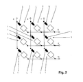
- FIG. 2 shows an exemplary embodiment of a direct converter according to the present disclosure.
- Exemplary embodiments of the present disclosure provide a method for operating a direct converter circuit, by means of which small energy fluctuations on phase modules can be achieved. Exemplary embodiments of the present disclosure also provide a device with which the method according to the disclosure can be carried out in a particularly simple manner.
- the direct converter circuit includes at least two phase modules and serves to connect phases of a first current system or voltage system to phases of a second current system or voltage system. Furthermore, each phase module includes a plurality of two-pole switching cells connected in series with one another, and each switching cell has controllable two-way power semiconductor switches with a controlled one-way current-carrying direction and a capacitive energy store. According to the method, the power semiconductor switches of the switching cells of the associated phase module are controlled by means of a control signal.
- each phase module has an inductor in series with the series circuit of the switching cells and, for each phase module, the control signal is formed from the difference between a reference signal in relation to the voltage over the phase module and a voltage signal over the inductor.
- the voltage signal over the inductor is formed from a reference signal in relation to the current through the phase module.
- the reference signal in relation to the current through the phase module is in turn formed from a mean value or instantaneous value of a phase power of a phase of the first current system or voltage system connected to the phase module, from a mean value or instantaneous value of a phase power of a phase of the second current system or voltage system connected to the phase module, from the sum of the instantaneous values or of the mean values of the phase powers of the phases of the first current system or voltage system and from the sum of the instantaneous values or of the mean values of the phase powers of the phases of the second power or voltage system.
- a distribution of all phase currents and currents of the capacitive energy store among the phase modules can advantageously be achieved, so that a low amplitude of the energy fluctuations on phase modules can be achieved, as a result of which a reliable and stable operation of the direct converter circuit can be achieved and the capacitive energy stores of the switching cells can be dimensioned as small and are therefore space-saving and economical.
- the control circuit is connected to the power semiconductor switches of the switching cells of the phase module.
- the difference between the reference signal in relation to the voltage over the phase module and the voltage signal over the inductor is fed to the control circuit to form the control signal.
- a common first calculation unit for the formation of the voltage signal over the inductor from the reference signal in relation to the current through the phase module is provided for all phase modules.
- a common second calculation unit is provided for all phase modules for the formation of the reference signal in relation to the current through the phase module from the mean value or instantaneous value of the phase power of the phase of the first current system or voltage system connected to the phase module, from the mean value or instantaneous value of the phase power of the phase of the second current system or voltage system connected to the phase module, from the sum of the instantaneous values or of the mean values of the phase powers of the phases of the first current system or voltage system and from the sum of the instantaneous values or of the mean values of the phase powers of the phases of the second current system or voltage system.
- the device according to the present disclosure for carrying out the method for operating the direct converter circuit can therefore be implemented very simply and economically, as the circuit cost can be kept extremely low and furthermore only a small number of components are required for its setup.
- the method according to the present disclosure can thus be carried out in a particularly simple manner by means of this device.
- FIG. 1 shows an exemplary embodiment of a device according to the present disclosure to carry out the method according to the present disclosure for the operation of a direct converter circuit. It is to be noted that only one phase module 1 of the direct converter circuit is shown in FIG. 1 for the sake of clarity.
- the direct converter circuit according to FIG. 1 generally includes at least two phase modules 1 , wherein each phase module 1 serves to connect phases U, V, W of a first current system or voltage system with phases R, S, T of a second current system or voltage system. It is assumed with regard to FIG. 1 that the first current system or voltage system has three phases U, V, W, and the second current system or voltage system similarly has three phases R, S, T, wherein any given number of phases is naturally conceivable with regard to the systems.
- Each phase module 1 includes a plurality of two-pole switching cells 2 connected in series with one another, wherein each switching cell 2 has controllable two-way power semiconductor switches with a controlled one-way current-carrying direction and a capacitive energy store.
- the respective controllable power semiconductor switch may be designed, for example, as a turn-off thyristor (GTO—Gate Turn-Off Thyristor) or as an integrated thyristor with a commutated control electrode (IGCT—Integrated Gate Commutated Thyristor) in each case with an antiparallel-switched diode.
- FIG. 2 shows an exemplary embodiment of a direct converter with the phase modules described above.
- the power semiconductor switches of the switching cells 2 are controlled by means of a control signal S 1 for each phase module 1 .
- the control signal S 1 may be temporarily offset for each switching cell 2 , so that each switching cell 2 can advantageously be controlled in a temporarily offset manner.
- each phase module 1 has an inductor L UR , L US , L UT ; L VR , L VS , L VT ; L WR , L WS , L WT in series with the series circuit of the switching cells, respectively, and, for each phase module 1 , the control signal S 1 is formed for each phase module 1 from the difference between a reference signal V ref,UR , V ref,US , V ref,UT , V ref,VR , V ref,VS , V ref,VT , V ref,WR , V ref,WS , V ref,WT in relation to the voltage U UR , U US , U UT ; U VR , U VS , U VT ; U WR , U WS , U WT over the phase module 1 and a voltage signal V LUR , V LUS , V LUT , V LVR , V LVS , V LVT , V LWR , V LWS , V LWT in relation to the voltage U UR
- the voltage signal V LUR , V LUS , V LUT , V LVR , V LVS , V LVT , V LWR , V LWS , V LWT over the inductor L UR , L US , L UT ; L VR , L VS , L VT ; L WR , L WS , L WT is formed from a reference signal i ref,UR , i ref,US , i ref,UT , i ref,VR , i ref,VS , i ref,VT , i ref,WR , i ref,WS , i ref,WT in relation to the current i UR , i US , i UT ; I VR , i VS , i VT ; i WR , i WS , i WT through the phase module 1 , respectively.
- the reference signal V ref,UR , V ref,US , V ref,UT , V ref,VR , V ref,VS , V ref,VT , V ref,WR , V ref,WS , V ref,WT in relation to the voltage U UR , U US , U UT ; U VR , U VS , U VT ; U WR , U WS , U WT over the phase module 1 may be generated by a higher-order current regulator for the phase currents of the phases U, V, W of the first current system or voltage system and by a higher-order current regulator for the phase currents of the phases R, S, T of the second current system or voltage system.
- the reference signal i ref,UR , i ref,US , i ref,UT , i ref,VR , i ref,VS , i ref,VT , i ref,WR , i ref,WS , i ref,WT in relation to the current i UR , i US , i UT ; i VR , i VS , i VT ; i WR , i WS , i WT through the phase module 1 is formed from a mean value P U , P V , P W or instantaneous value P U , P V , P W of a phase power of a phase U, V, W of the first current system or voltage system connected to the phase module 1 , from a mean value P R , P S , P T or instantaneous value P R , P S , P T of a phase power of a phase R, S, T of the second current system or voltage system connected to the phase module 1 , from the sum of
- V LXY L XY ⁇ ⁇ ⁇ t ⁇ i ref , XY , [ 1 ]
- the index XY generally indicates the connection of a phase X of the first current system or voltage system to a phase Y of the second current system or voltage system.
- the voltage signal V LXY over the inductor L XY of the associated phase module 1 can also be formed, for example, by a feedback:
- V LXY K ( i ref,XY ⁇ i XY ) [1a],
- K is a selectable factor
- the power semiconductor switches of each switching cell 2 are connected in the manner of a bridge circuit, wherein the capacitive energy store is connected in parallel with the bridge circuit.
- the power semiconductor switches of each switching cell 2 in the manner of a half-bridge circuit, wherein the capacitive energy store is then connected in parallel with the half-bridge circuit.
- the reference signal i ref,UR , i ref,US , i ref,UT , i ref,VR , i ref,VS , i ref,VT , i ref,WR , i ref,WS , i ref,WT in relation to the current i UR , i US , i UT ; i VR , i VS , i VT ; i WR , i WS , i WT through the phase module 1 is additionally formed from a phase current i U , i V , i W of the phase U, V, W of the first current system or voltage system connected to the phase module 1 and from a phase current i R , i S , i T of the phase R, S, T of the second current system or voltage system connected to the phase module 1 .
- the reference signal i ref,XY in relation to the current i XY through the phase module 1 is therefore generally formed by the following formula:
- index X is a phase of the first current system or voltage system
- index Y is a phase of the second current system or voltage system
- P X , P Y are the mean values of the phase powers P X
- P Y and P 1M is the sum of the mean values of the phase powers of the first current system or voltage system
- P 2M is the sum of the mean values of the phase powers of the second current system or voltage system.
- the reference signal i ref,XY in relation to the current i XY through the phase module 1 is formed by the following formula:
- index X is again a phase of the first current system or voltage system
- index Y is a phase of the second current system or voltage system
- P X , P Y are the instantaneous values of the phase powers
- P 1 is the sum of the instantaneous values of the phase powers of the first current system or voltage system
- P 2 is the sum of the mean values of the phase powers of the second current system or voltage system.
- the respective phase current i U , i V , i W of the phase U, V, W of the first current system or voltage system connected to the phase module 1 and the respective phase current i R , i S , i T of the phase R, S, T of the second current system or voltage system connected to the phase module 1 may be an instantaneous value, which is determined, for example, through measurement.
- the instantaneous value of the phase power P U , P V , P W of the phase U, V, W of the first current system or voltage system connected to the phase module 1 is formed, for example, from a reference signal I ref,U , I ref,V , I ref,W in relation to the phase current i U , i V , i W of the phase U, V, W of the first current system or voltage system and from a reference signal V ref,U , V ref,V , V ref,W in relation to a phase voltage u U , u V , u W of the phase U, V, W of the first current system or voltage system connected to the phase module 1 .
- the instantaneous value of the phase power P U , P V , P W of the phase U, V, W of the first current system or voltage system connected to the phase module 1 is formed, for example, from the phase current i U , i V , i W , for example from a measurement value, of the phase U, V, W of the first current system or voltage system connected to the phase module 1 and from a phase voltage u U , u V , u W , for example from a measurement value, of the phase U, V, W of the first current system or voltage system connected to the phase module 1 .
- the instantaneous value of the phase power P R , P S , P T of the phase R, S, T of the second current system or voltage system connected to the phase module 1 is formed, for example, from a reference signal I ref,R , I ref,S , I ref,T in relation to the phase current i R , i S , i T of the phase R, S, T of the second current system or voltage system connected to the phase module 1 and from a reference signal V ref,R , V ref,S , V ref,T in relation to a phase voltage U R , U S , U T of the phase R, S, T of the second current system or voltage system connected to the phase module 1 .
- the instantaneous value of the phase power P R , P S , P T of the phase R, S, T of the second current system or voltage system connected to the phase module 1 is formed, for example, from the phase current i R , i S , i T , for example from a measurement value, of the phase R, S, T of the second current system or voltage system connected to the phase module 1 and from a phase voltage u R , u S , u T , for example from a measurement value, of the phase R, S, T of the second current system or voltage system connected to the phase module 1 .
- the respective instantaneous value of the phase power P U , P V , P W of the phase U, V, W of the first current system or voltage system connected to the phase module 1 and the respective instantaneous value of the phase power P R , P S , P T of the phase R, S, T of the second current system or voltage system connected to the phase module 1 is calculated in particular according to formula [3a]:
- index X is a phase of the first current system or voltage system
- index Y is a phase of the second current system or voltage system
- the reference signal I ref,U , I ref,V , I ref,W in relation to the phase current i U , i V , i W of the phase U, V, W of the first current system or voltage system connected to the phase module 1 or generally I ref,X
- the reference signal V ref,U , V ref,V , V ref,W in relation to the phase voltage u U , u V , u W of the phase U, V, W of the first current system or voltage system connected to the phase module 1 or generally V ref,X
- the reference signal I ref,R , I ref,S , I ref,T in relation to the phase current i R , i R , i T of the phase R, S, T of the second current system or voltage system connected to the phase module 1 or generally I ref,Y and the reference signal V ref,R , V ref,S , V ref,T in relation to the phase voltage u R , u S , u T of the phase R, S, T of the second current system
- the respective instantaneous value of the phase power P U , P V , P W of the phase U, V, W of the first current system or voltage system connected to the phase module 1 and the respective instantaneous value of the phase power P R , P S , P T of the phase R, S, T of the second current system or voltage system connected to the phase module 1 is calculated from the aforementioned measurement values according to formula [3b].
- index X is a phase of the first current system or voltage system
- index Y is a phase of the second current system or voltage system
- the device according to the disclosure for carrying out the method for operating a direct converter circuit includes a control circuit 3 for each phase module 1 serving to generate the control signal S 1 .
- the control circuit 3 is connected to the power semiconductor switches of the switching cells 2 of the phase module 1 .
- a common first calculation unit 4 is provided to form the voltage signal V LUR , V LUS , V LUT , V LVR , V LVS , V LVT , V LWR , V LWS , V LWT over the inductor L UR , L US , L UT ; L VR , L VS , L VT ; L WR , L WS , L WT , in particular according to formula [1], from the reference signal i ref,UR , i ref,US , i ref,UT , i ref,VR , I ref,VS , i ref,VT , i ref,WR , i ref,WS , i ref,WT in relation to the current i UR , i US , i UT ; i VR , i VS , i VT ; i WR , i WS , i WT through the phase module 1 , respectively.
- a common second calculation unit 5 is provided for all phase modules 1 to form the reference signal i ref,UR , i ref,US , i ref,UT , i ref,VR , i ref,VS , i ref,VT , i ref,WR , i ref,WS , i ref,WT in relation to the current i UR , i US , i UT ; i VR , i VS , i VT ; i WR , i WS , i WT through the phase module 1 , in particular according to formula [2a] or [2b], from the mean value P U , P V , P W or instantaneous value P U , P V , P W of the phase power of the phase U, V, W of the first current system or voltage system connected to the phase module 1 , from the mean value P R , P S , P T or instantaneous value P R , P S , P T of the phase power of the phase R
- the common second calculation unit 5 forms the reference signal i ref,UR , i ref,US , i ref,UT , i ref,VR , i ref,VS , i ref,VT , i ref,WR , i ref,WS , i ref,WT in relation to the current i UR , i US , i UT ; i VR , i VS , i VT ; i WR , i WS , i WT through the phase module 1 , in particular according to formula [2a] or [2b], additionally from the phase current i U , i V , i W of the phase U, V, W of the first current system or voltage system connected to the phase module 1 and from the phase current i R , i S , i T of the phase R, S, T of the second current system or voltage connected to the phase module 1 .
- a common third calculation unit 6 is provided for all phase modules 1 to form the instantaneous value of the phase power P U , P V , P W of the phase U, V, W of the first current system or voltage system connected to the phase module 1 , in particular according to formula [3a], from the reference signal I ref,U , I ref,V , I ref,W in relation to the phase current i U , i V , i W of the phase U, V, W of the first current system or voltage system connected to the phase module 1 and from the reference signal V ref,U , V ref,V , V ref,W in relation to the phase voltage u U , u V , u W of the phase U, V, W of the first current system or voltage system connected to the phase module 1 and to form the instantaneous value of the phase power P R , P S , P T of the phase R, S, T of the second current system or voltage system connected to the phase module 1 , in particular according to formula [3a], from the reference signal
- a common third calculation unit 6 is provided for all phase modules 1 to form the instantaneous value of the phase power P U , P V , P W of the phase U, V, W of the first current system or voltage system connected to the phase module 1 , in particular according to formula [3b], from the phase current i U , i V , i W of the phase U, V, W of the first current system or voltage system connected to the phase module 1 and from the phase voltage u U , u V , u W of the phase U, V, W of the first current system or voltage system connected to the phase module 1 and to form the instantaneous value of the phase power P R , P S , P T of the phase R, S, T of the second current system or voltage system connected to the phase module 1 , in particular according to formula [3b], from the phase current i R , i S , i T of the phase R, S, T of the second current system or voltage system connected to the phase module 1 and from a phase voltage u R
Abstract
Description
- This application claims priority as a continuation application under 35 U.S.C. §120 to PCT/EP2010/069277, which was filed as an International Application on Dec. 9, 2010 designating the U.S., and which claims priority to European Application 09179643.3 filed in Europe on Dec. 17, 2009. The entire contents of these applications are hereby incorporated by reference in their entireties.
- The present disclosure relates to the field of power electronics. More particularly, the present disclosure relates to a method for operating a direct converter circuit, and to a device to carry out the method.
- In the past, direct converter circuits, such as matrix converters, tended to be of academic importance. Today, however, direct converter circuits are gaining in importance, particularly for industrial applications, because an input voltage or an input current of a first amplitude and a first frequency can be converted directly into an output voltage or into an output current of a second amplitude and a second frequency by means of a direct converter circuit with no expensive intermediate direct voltage circuit or intermediate direct current circuit. A direct converter circuit of this type is disclosed, for example, in U.S. Pat. No. 6,900,998 B2. Here, the direct converter circuit has n=3 input phase connections and p=3 output phase connections, i.e. the direct converter circuit from U.S. Pat. No. 6,900,998 B2 has a three-phase design on the input side and on the output side. The direct converter circuit from U.S. Pat. No. 6,900,998 B2 furthermore includes nine phase modules, each with a two-pole switching cell to switch a positive and a negative voltage between the poles, wherein each output phase connection is connected in series with each input phase connection in each case directly via a switching cell. A switching cell of this type has controllable two-way power semiconductor switches with a controlled one-way current-carrying direction and a capacitive energy store.
- A drawback with a direct converter circuit according to U.S. Pat. No. 6,900,998 B2 is that the voltage on each branch, i.e. on each phase module, cannot be set in such a way that a continuous current flow can be achieved by the switching cells, as a result of which no active current setting by the respective branch is possible. As a result, only a very restricted or no exchange of electrical energy between individual branches is possible with the direct converter circuit from U.S. Pat. No. 6,900,998 B2. However, if the direct converter circuit is intended to be capable of transferring a large amount of electrical energy, the capacitors of the switching cells from U.S. Pat. No. 6,900,998 B2 must be dimensioned as correspondingly large, resulting in an enormous space requirement of a direct converter circuit of this type and considerable costs. As a result, systems set up with direct converter circuits of this type will similarly have correspondingly substantial space requirements and will be correspondingly expensive.
- Energy fluctuations in the individual phase modules result in voltage fluctuations in the capacitive energy stores in the associated switching cells. However, for a reliable and stable operation, and in order to enable a low-cost implementation of the direct converter circuit, it must be possible to limit and minimize the amplitude of this energy fluctuation on the phase module in order to be able to limit the maximum voltage on each individual capacitive energy store of the associated switching cell of the phase module to a required value with the smallest possible capacitive energy store.
- In “A Methodology for Developing ‘Chainlink’ Converters”, EPE 8 Sep. 2009, a direct converter circuit is disclosed in which each phase module has an inductor in series with the series circuit of the switching cells.
- In WO 2008/067788 A1, a method is disclosed for the operation of a converter circuit according to WO 2007/023064 A1, which regulates the energy content of the switching cells. The method described in WO 2008/067788 A1 applies only to designs of the converter circuit according to WO 2007/023064 A1 which connect three phases of one system to two phases of another system, wherein the currents in the connection terminals of the direct converter circuits are always zero.
- In “On Dynamics and Voltage Control of the Modular Multilevel Converter”, EPE 8 Sep. 2009, a method is disclosed for the operation of a converter circuit, in which the balancing of the phase modules is effected with the aid of a control provided specifically for that purpose.
- An exemplary embodiment of the present disclosure provides a method for operating a direct converter circuit. The direct converter circuit includes at least two phase modules and is configured to connect phases of a first current system or voltage system with phases of a second current system or voltage system. Each phase module respectively includes a plurality of two-pole switching cells connected in series with one another. Each phase module includes an inductor respectively in series with the series circuit of the corresponding switching cells, and each switching cell having controllable two-way power semiconductor switches with a controlled one-way current-carrying direction and a capacitive energy store. The exemplary method includes controlling the power semiconductor switches of the switching cells of the associated phase module by means of a control signal. For each phase module, the exemplary method includes forming the control signal from the difference between a reference signal in relation to a voltage over the phase module and a voltage signal over the inductor, respectively. The exemplary method includes forming the voltage signal over the inductor from a reference signal in relation to the current through the corresponding phase module, respectively. In addition, the exemplary method includes forming the reference signal in relation to the current through the corresponding phase module from a mean value or instantaneous value of a phase power of a phase of the first current system or voltage system connected to the phase module, from a mean value or instantaneous value of a phase power of a phase of the second current system or voltage system connected to the corresponding phase module, from the sum of the instantaneous values or of the mean values of the phase powers of the phases of the first current system or voltage system, and from the sum of the instantaneous values or of the mean values of the phase powers of the phases of the second current system or voltage system, respectively.
- An exemplary embodiment of the present disclosure provides a device for operating a direct converter circuit. The direct converter circuit includes at least two phase modules and is configured to connect phases of a first current system or voltage system with phases of a second current system or voltage system. Each phase module respectively includes a plurality of two-pole switching cells connected in series with one another. Each phase module respectively includes an inductor in series with the series circuit of the switching cells. Each switching cell includes controllable two-way power semiconductor switches with a controlled one-way current-carrying direction and a capacitive energy store. The exemplary device includes a control circuit for each phase module configured to generate a control signal. The control circuit is connected to the power semiconductor switches of the switching cells of the corresponding phase module, respectively. In relation to each phase module, the difference between a reference signal in relation to the voltage over the corresponding phase module and a voltage signal over the inductor is fed to the control circuit to form the control signal, respectively. The exemplary device also includes, for all phase modules, a common first calculation unit configured to form the voltage signal over the inductor from a reference signal in relation to the current through the corresponding phase module, respectively. In addition, the exemplary device includes, for all phase modules, a common second calculation unit configured to form the reference signal in relation to the current through the corresponding phase module from a mean value or instantaneous value of a phase power of a phase of the first current system or voltage system connected to the corresponding phase module, from a mean value or instantaneous value of a phase power of a phase of the second current system or voltage system connected to the corresponding phase module, from the sum of the instantaneous values or of the mean values of the phase powers of the phases of the first current system or voltage system, and from the sum of the instantaneous values or of the mean values of the phase powers of the phases of the second current system or voltage system, respectively.
- Additional refinements, advantages and features of the present disclosure are described in more detail below with reference to exemplary embodiments illustrated in the drawings, in which:
-
FIG. 1 shows an exemplary embodiment of a device according to the present disclosure to carry out the method according to the present disclosure for operating a direct converter circuit, and -
FIG. 2 shows an exemplary embodiment of a direct converter according to the present disclosure. - The reference numbers used in the drawing and their meanings are summarized in the reference number list. In the drawings, the same parts are essentially provided with the same reference numbers. The embodiments described serve as examples of the subject-matter of the disclosure and have no limiting effect.
- Exemplary embodiments of the present disclosure provide a method for operating a direct converter circuit, by means of which small energy fluctuations on phase modules can be achieved. Exemplary embodiments of the present disclosure also provide a device with which the method according to the disclosure can be carried out in a particularly simple manner.
- The direct converter circuit includes at least two phase modules and serves to connect phases of a first current system or voltage system to phases of a second current system or voltage system. Furthermore, each phase module includes a plurality of two-pole switching cells connected in series with one another, and each switching cell has controllable two-way power semiconductor switches with a controlled one-way current-carrying direction and a capacitive energy store. According to the method, the power semiconductor switches of the switching cells of the associated phase module are controlled by means of a control signal. According to the an exemplary embodiment of the present disclosure, each phase module has an inductor in series with the series circuit of the switching cells and, for each phase module, the control signal is formed from the difference between a reference signal in relation to the voltage over the phase module and a voltage signal over the inductor. The voltage signal over the inductor is formed from a reference signal in relation to the current through the phase module. The reference signal in relation to the current through the phase module is in turn formed from a mean value or instantaneous value of a phase power of a phase of the first current system or voltage system connected to the phase module, from a mean value or instantaneous value of a phase power of a phase of the second current system or voltage system connected to the phase module, from the sum of the instantaneous values or of the mean values of the phase powers of the phases of the first current system or voltage system and from the sum of the instantaneous values or of the mean values of the phase powers of the phases of the second power or voltage system.
- Due to the mean value or instantaneous value of the phase power of the phase of the first current system or voltage system connected to the phase module, the mean value or instantaneous value of the phase power of the phase of the second current system or voltage system connected to the phase module, the sum of the instantaneous values or of the mean values of the phase powers of the phases of the first current system or voltage system and the sum of the instantaneous values or of the mean values of the phase powers of the phases of the second current system or voltage system is ultimately incorporated into the formation of the control signal, a distribution of all phase currents and currents of the capacitive energy store among the phase modules can advantageously be achieved, so that a low amplitude of the energy fluctuations on phase modules can be achieved, as a result of which a reliable and stable operation of the direct converter circuit can be achieved and the capacitive energy stores of the switching cells can be dimensioned as small and are therefore space-saving and economical.
- The device according to the present disclosure for carrying out the method for operating the direct converter circuit includes a control circuit for each phase module serving to generate the control signal. The control circuit is connected to the power semiconductor switches of the switching cells of the phase module. In relation to each phase module, the difference between the reference signal in relation to the voltage over the phase module and the voltage signal over the inductor is fed to the control circuit to form the control signal. Furthermore, a common first calculation unit for the formation of the voltage signal over the inductor from the reference signal in relation to the current through the phase module is provided for all phase modules. In addition, a common second calculation unit is provided for all phase modules for the formation of the reference signal in relation to the current through the phase module from the mean value or instantaneous value of the phase power of the phase of the first current system or voltage system connected to the phase module, from the mean value or instantaneous value of the phase power of the phase of the second current system or voltage system connected to the phase module, from the sum of the instantaneous values or of the mean values of the phase powers of the phases of the first current system or voltage system and from the sum of the instantaneous values or of the mean values of the phase powers of the phases of the second current system or voltage system.
- The device according to the present disclosure for carrying out the method for operating the direct converter circuit can therefore be implemented very simply and economically, as the circuit cost can be kept extremely low and furthermore only a small number of components are required for its setup. The method according to the present disclosure can thus be carried out in a particularly simple manner by means of this device.
-
FIG. 1 shows an exemplary embodiment of a device according to the present disclosure to carry out the method according to the present disclosure for the operation of a direct converter circuit. It is to be noted that only onephase module 1 of the direct converter circuit is shown inFIG. 1 for the sake of clarity. The direct converter circuit according toFIG. 1 generally includes at least twophase modules 1, wherein eachphase module 1 serves to connect phases U, V, W of a first current system or voltage system with phases R, S, T of a second current system or voltage system. It is assumed with regard toFIG. 1 that the first current system or voltage system has three phases U, V, W, and the second current system or voltage system similarly has three phases R, S, T, wherein any given number of phases is naturally conceivable with regard to the systems. Eachphase module 1 includes a plurality of two-pole switching cells 2 connected in series with one another, wherein each switchingcell 2 has controllable two-way power semiconductor switches with a controlled one-way current-carrying direction and a capacitive energy store. The respective controllable power semiconductor switch may be designed, for example, as a turn-off thyristor (GTO—Gate Turn-Off Thyristor) or as an integrated thyristor with a commutated control electrode (IGCT—Integrated Gate Commutated Thyristor) in each case with an antiparallel-switched diode. However, it is also conceivable to design a controllable power semiconductor switch, for example, as a power MOSFET with an additionally antiparallel-connected diode or as a bipolar transistor with a gate electrode (IGBT) disposed in isolation with an additionally antiparallel-connected diode.FIG. 2 shows an exemplary embodiment of a direct converter with the phase modules described above. - According to an exemplary embodiment of the present disclosure, the power semiconductor switches of the
switching cells 2 are controlled by means of a control signal S1 for eachphase module 1. The control signal S1 may be temporarily offset for each switchingcell 2, so that each switchingcell 2 can advantageously be controlled in a temporarily offset manner. According to an exemplary embodiment of the present disclosure, eachphase module 1 has an inductor LUR, LUS, LUT; LVR, LVS, LVT; LWR, LWS, LWT in series with the series circuit of the switching cells, respectively, and, for eachphase module 1, the control signal S1 is formed for eachphase module 1 from the difference between a reference signal Vref,UR, Vref,US, Vref,UT, Vref,VR, Vref,VS, Vref,VT, Vref,WR, Vref,WS, Vref,WT in relation to the voltage UUR, UUS, UUT; UVR, UVS, UVT; UWR, UWS, UWT over thephase module 1 and a voltage signal VLUR, VLUS, VLUT, VLVR, VLVS, VLVT, VLWR, VLWS, VLWT over the inductor LUR, LUS, LUT; LVR, LVS, LVT; LWR, LWS, LWT, respectively. The voltage signal VLUR, VLUS, VLUT, VLVR, VLVS, VLVT, VLWR, VLWS, VLWT over the inductor LUR, LUS, LUT; LVR, LVS, LVT; LWR, LWS, LWT is formed from a reference signal iref,UR, iref,US, iref,UT, iref,VR, iref,VS, iref,VT, iref,WR, iref,WS, iref,WT in relation to the current iUR, iUS, iUT; IVR, iVS, iVT; iWR, iWS, iWT through thephase module 1, respectively. The reference signal Vref,UR, Vref,US, Vref,UT, Vref,VR, Vref,VS, Vref,VT, Vref,WR, Vref,WS, Vref,WT in relation to the voltage UUR, UUS, UUT; UVR, UVS, UVT; UWR, UWS, UWT over thephase module 1 may be generated by a higher-order current regulator for the phase currents of the phases U, V, W of the first current system or voltage system and by a higher-order current regulator for the phase currents of the phases R, S, T of the second current system or voltage system. Furthermore, the reference signal iref,UR, iref,US, iref,UT, iref,VR, iref,VS, iref,VT, iref,WR, iref,WS, iref,WT in relation to the current iUR, iUS, iUT; iVR, iVS, iVT; iWR, iWS, iWT through thephase module 1 is formed from a mean valueP U,P V,P W or instantaneous value PU, PV, PW of a phase power of a phase U, V, W of the first current system or voltage system connected to thephase module 1, from a mean valueP R,P S,P T or instantaneous value PR, PS, PT of a phase power of a phase R, S, T of the second current system or voltage system connected to thephase module 1, from the sum of the instantaneous values PUVW or of the mean values PUVWM of the phase powers of the phases U, V, W of the first current system or voltage system and from the sum of the instantaneous values PRST or of the mean values PRSTM of the phase powers of the phases R, S, T of the second current system or voltage system. - Due to the mean value
P U,P V,P W or instantaneous value PU, PV, PW of the phase power of the phase U, V, W of the first current system or voltage system connected to thephase module 1, the mean valueP R,P S,P T or instantaneous value PR, PS, PT of the phase power of the phase R, S, T of the second current system or voltage system connected to thephase module 1, the sum of the instantaneous values PUVW or of the mean values PUVWM of the phase powers of the phases U, V, W of the first current system or voltage system and the sum of the instantaneous values PRST or of the mean values PRSTM of the phase powers of the phases R, S, T of the second current system or voltage system is ultimately incorporated into the formation of the control signal S1, a distribution of all phase currents and currents of the capacitive energy store among thephase modules 1 can advantageously be achieved, so that a required low amplitude of the energy fluctuations onphase modules 1 can be achieved, as a result of which a reliable and stable operation of the direct converter circuit can be achieved and the capacitive energy stores of theswitching cells 2 can be dimensioned as small and are therefore space-saving and economical. - The following formula is generally used to form the voltage signal VLXY over the inductor LXY of the associated phase module 1:
-
- where the index XY generally indicates the connection of a phase X of the first current system or voltage system to a phase Y of the second current system or voltage system. Alternatively, the voltage signal VLXY over the inductor LXY of the associated
phase module 1 can also be formed, for example, by a feedback: -
V LXY =K(i ref,XY −i XY) [1a], - where K is a selectable factor.
- According to the exemplary embodiment illustrated in
FIG. 1 , the power semiconductor switches of each switchingcell 2 are connected in the manner of a bridge circuit, wherein the capacitive energy store is connected in parallel with the bridge circuit. Alternatively, however, it would also be conceivable to connect the power semiconductor switches of each switchingcell 2 in the manner of a half-bridge circuit, wherein the capacitive energy store is then connected in parallel with the half-bridge circuit. - For each
phase module 1, the reference signal iref,UR, iref,US, iref,UT, iref,VR, iref,VS, iref,VT, iref,WR, iref,WS, iref,WT in relation to the current iUR, iUS, iUT; iVR, iVS, iVT; iWR, iWS, iWT through thephase module 1 is additionally formed from a phase current iU, iV, iW of the phase U, V, W of the first current system or voltage system connected to thephase module 1 and from a phase current iR, iS, iT of the phase R, S, T of the second current system or voltage system connected to thephase module 1. - The reference signal iref,XY in relation to the current iXY through the
phase module 1 is therefore generally formed by the following formula: -
- where generally the index X is a phase of the first current system or voltage system, the index Y is a phase of the second current system or voltage system,
P X,P Y are the mean values of the phase powers PX, PY and P1M is the sum of the mean values of the phase powers of the first current system or voltage system, and P2M is the sum of the mean values of the phase powers of the second current system or voltage system. - Alternatively, it is also conceivable that the reference signal iref,XY in relation to the current iXY through the
phase module 1 is formed by the following formula: -
- where generally the index X is again a phase of the first current system or voltage system, the index Y is a phase of the second current system or voltage system, PX, PY are the instantaneous values of the phase powers and P1 is the sum of the instantaneous values of the phase powers of the first current system or voltage system, and P2 is the sum of the mean values of the phase powers of the second current system or voltage system.
- The respective phase current iU, iV, iW of the phase U, V, W of the first current system or voltage system connected to the
phase module 1 and the respective phase current iR, iS, iT of the phase R, S, T of the second current system or voltage system connected to thephase module 1 may be an instantaneous value, which is determined, for example, through measurement. - For each
phase module 1, the instantaneous value of the phase power PU, PV, PW of the phase U, V, W of the first current system or voltage system connected to thephase module 1 is formed, for example, from a reference signal Iref,U, Iref,V, Iref,W in relation to the phase current iU, iV, iW of the phase U, V, W of the first current system or voltage system and from a reference signal Vref,U, Vref,V, Vref,W in relation to a phase voltage uU, uV, uW of the phase U, V, W of the first current system or voltage system connected to thephase module 1. Alternatively, however, it is also conceivable that the instantaneous value of the phase power PU, PV, PW of the phase U, V, W of the first current system or voltage system connected to thephase module 1 is formed, for example, from the phase current iU, iV, iW, for example from a measurement value, of the phase U, V, W of the first current system or voltage system connected to thephase module 1 and from a phase voltage uU, uV, uW, for example from a measurement value, of the phase U, V, W of the first current system or voltage system connected to thephase module 1. - In addition, the instantaneous value of the phase power PR, PS, PT of the phase R, S, T of the second current system or voltage system connected to the
phase module 1 is formed, for example, from a reference signal Iref,R, Iref,S, Iref,T in relation to the phase current iR, iS, iT of the phase R, S, T of the second current system or voltage system connected to thephase module 1 and from a reference signal Vref,R, Vref,S, Vref,T in relation to a phase voltage UR, US, UT of the phase R, S, T of the second current system or voltage system connected to thephase module 1. Alternatively, it is also conceivable that the instantaneous value of the phase power PR, PS, PT of the phase R, S, T of the second current system or voltage system connected to thephase module 1 is formed, for example, from the phase current iR, iS, iT, for example from a measurement value, of the phase R, S, T of the second current system or voltage system connected to thephase module 1 and from a phase voltage uR, uS, uT, for example from a measurement value, of the phase R, S, T of the second current system or voltage system connected to thephase module 1. - The respective instantaneous value of the phase power PU, PV, PW of the phase U, V, W of the first current system or voltage system connected to the
phase module 1 and the respective instantaneous value of the phase power PR, PS, PT of the phase R, S, T of the second current system or voltage system connected to thephase module 1 is calculated in particular according to formula [3a]: -
P X =V ref,X ·I ref,X -
P Y =V ref,Y ·I ref,Y [3a], - where again generally the index X is a phase of the first current system or voltage system, and the index Y is a phase of the second current system or voltage system.
- The reference signal Iref,U, Iref,V, Iref,W in relation to the phase current iU, iV, iW of the phase U, V, W of the first current system or voltage system connected to the
phase module 1 or generally Iref,X, the reference signal Vref,U, Vref,V, Vref,W in relation to the phase voltage uU, uV, uW of the phase U, V, W of the first current system or voltage system connected to thephase module 1 or generally Vref,X, the reference signal Iref,R, Iref,S, Iref,T in relation to the phase current iR, iR, iT of the phase R, S, T of the second current system or voltage system connected to thephase module 1 or generally Iref,Y and the reference signal Vref,R, Vref,S, Vref,T in relation to the phase voltage uR, uS, uT of the phase R, S, T of the second current system or voltage system connected to thephase module 1 or generally Vref,Y is in each case pre-definable. - Alternatively, it is also possible that the respective instantaneous value of the phase power PU, PV, PW of the phase U, V, W of the first current system or voltage system connected to the
phase module 1 and the respective instantaneous value of the phase power PR, PS, PT of the phase R, S, T of the second current system or voltage system connected to thephase module 1 is calculated from the aforementioned measurement values according to formula [3b]. -
P X =u X ·i X -
P Y =u Y ·i Y [3b], - where again generally the index X is a phase of the first current system or voltage system, and the index Y is a phase of the second current system or voltage system.
- It should be explicitly stated that the aforementioned formation of the above-mentioned instantaneous values PU, PV, PW, PR, PS, PT of the phase powers can also be effected in other ways.
- According to the exemplary embodiment illustrated in
FIG. 1 , the device according to the disclosure for carrying out the method for operating a direct converter circuit includes acontrol circuit 3 for eachphase module 1 serving to generate the control signal S1. Thecontrol circuit 3 is connected to the power semiconductor switches of theswitching cells 2 of thephase module 1. According to an exemplary embodiment of the present disclosure, in relation to eachphase module 1, the difference between the reference signal Vref,UR, Vref,US, Vref,UT, Vref,VR, Vref,VS, Vref,VT, Vref,WR, Vref,WS, Vref,WT in relation to the voltage UUR, UUS, UUT; UVR, UVS, UVT; UWR, UWS, UWT over thephase module 1 and a voltage signal VLUR, VLUS, VLUT, VLVR, VLVS, VLVT, VLWR, VLWS, VLWT over the inductor LUR, LUS, LUT; LVR, LVS, LVT; LWR, LWS, LWT is fed to thecontrol circuit 3 to form the control signal S1, respectively. Furthermore, for allphase modules 1, a commonfirst calculation unit 4 is provided to form the voltage signal VLUR, VLUS, VLUT, VLVR, VLVS, VLVT, VLWR, VLWS, VLWT over the inductor LUR, LUS, LUT; LVR, LVS, LVT; LWR, LWS, LWT, in particular according to formula [1], from the reference signal iref,UR, iref,US, iref,UT, iref,VR, Iref,VS, iref,VT, iref,WR, iref,WS, iref,WT in relation to the current iUR, iUS, iUT; iVR, iVS, iVT; iWR, iWS, iWT through thephase module 1, respectively. Furthermore, a commonsecond calculation unit 5 is provided for allphase modules 1 to form the reference signal iref,UR, iref,US, iref,UT, iref,VR, iref,VS, iref,VT, iref,WR, iref,WS, iref,WT in relation to the current iUR, iUS, iUT; iVR, iVS, iVT; iWR, iWS, iWT through thephase module 1, in particular according to formula [2a] or [2b], from the mean valueP U,P V,P W or instantaneous value PU, PV, PW of the phase power of the phase U, V, W of the first current system or voltage system connected to thephase module 1, from the mean valueP R,P S,P T or instantaneous value PR, PS, PT of the phase power of the phase R, S, T of the second current system or voltage system connected to thephase module 1, from the sum of the instantaneous values PUVW or of the mean values PUVWM of the phase powers of the phases U, V, W of the first current system or voltage system and from the sum of the instantaneous values PRST or of the mean values PRSTM of the phase powers of the phases R, S, T of the second current system or voltage system, respectively. - The common
second calculation unit 5 forms the reference signal iref,UR, iref,US, iref,UT, iref,VR, iref,VS, iref,VT, iref,WR, iref,WS, iref,WT in relation to the current iUR, iUS, iUT; iVR, iVS, iVT; iWR, iWS, iWT through thephase module 1, in particular according to formula [2a] or [2b], additionally from the phase current iU, iV, iW of the phase U, V, W of the first current system or voltage system connected to thephase module 1 and from the phase current iR, iS, iT of the phase R, S, T of the second current system or voltage connected to thephase module 1. - In addition, a common third calculation unit 6 is provided for all phase modules 1 to form the instantaneous value of the phase power PU, PV, PW of the phase U, V, W of the first current system or voltage system connected to the phase module 1, in particular according to formula [3a], from the reference signal Iref,U, Iref,V, Iref,W in relation to the phase current iU, iV, iW of the phase U, V, W of the first current system or voltage system connected to the phase module 1 and from the reference signal Vref,U, Vref,V, Vref,W in relation to the phase voltage uU, uV, uW of the phase U, V, W of the first current system or voltage system connected to the phase module 1 and to form the instantaneous value of the phase power PR, PS, PT of the phase R, S, T of the second current system or voltage system connected to the phase module 1, in particular according to formula [3a], from the reference signal Iref,R, Iref,S, Iref,T in relation to the phase current iR, iR, iT of the phase R, S, T of the second current system or voltage system connected to the phase module 1 and from a reference signal Vref,R, Vref,S, Vref,T in relation to the phase voltage uR, uS, uT of the phase R, S, T of the second current system or voltage system connected to the phase module 1, respectively.
- Alternatively, a common
third calculation unit 6 is provided for allphase modules 1 to form the instantaneous value of the phase power PU, PV, PW of the phase U, V, W of the first current system or voltage system connected to thephase module 1, in particular according to formula [3b], from the phase current iU, iV, iW of the phase U, V, W of the first current system or voltage system connected to thephase module 1 and from the phase voltage uU, uV, uW of the phase U, V, W of the first current system or voltage system connected to thephase module 1 and to form the instantaneous value of the phase power PR, PS, PT of the phase R, S, T of the second current system or voltage system connected to thephase module 1, in particular according to formula [3b], from the phase current iR, iS, iT of the phase R, S, T of the second current system or voltage system connected to thephase module 1 and from a phase voltage uR, uS, uT of the phase R, S, T of the second current system or voltage system connected to thephase module 1. - In total, it has been possible to show that the exemplary devices according to the disclosure, for example, according to
FIG. 1 , to carry out the method according to the disclosure for operating the direct converter circuit can be implemented very simply and economically, since the circuit outlay is extremely low and furthermore only a small number of components are required for the set-up. The method according to the disclosure can therefore be particularly simply carried out with these devices. -
- 1 Phase module
- 2 Switching cell
- 3 Control circuit
- 4 first calculation unit
- 5 second calculation unit
- 6 third calculation unit
Claims (8)
Applications Claiming Priority (4)
| Application Number | Priority Date | Filing Date | Title |
|---|---|---|---|
| EP09179643 | 2009-12-17 | ||
| EP09179643.3 | 2009-12-17 | ||
| EP09179643 | 2009-12-17 | ||
| PCT/EP2010/069277 WO2011082935A1 (en) | 2009-12-17 | 2010-12-09 | Method for operating a direct converter circuit and device for carrying out the method |
Related Parent Applications (1)
| Application Number | Title | Priority Date | Filing Date |
|---|---|---|---|
| PCT/EP2010/069277 Continuation WO2011082935A1 (en) | 2009-12-17 | 2010-12-09 | Method for operating a direct converter circuit and device for carrying out the method |
Publications (2)
| Publication Number | Publication Date |
|---|---|
| US20120249113A1 true US20120249113A1 (en) | 2012-10-04 |
| US8687397B2 US8687397B2 (en) | 2014-04-01 |
Family
ID=42199660
Family Applications (1)
| Application Number | Title | Priority Date | Filing Date |
|---|---|---|---|
| US13/526,048 Expired - Fee Related US8687397B2 (en) | 2009-12-17 | 2012-06-18 | Method for operating a direct converter circuit and device to carry out the method |
Country Status (12)
| Country | Link |
|---|---|
| US (1) | US8687397B2 (en) |
| EP (1) | EP2514087B1 (en) |
| JP (1) | JP5752704B2 (en) |
| KR (1) | KR101628431B1 (en) |
| CN (1) | CN102754323B (en) |
| BR (1) | BR112012014835A2 (en) |
| CA (1) | CA2783184A1 (en) |
| DK (1) | DK2514087T3 (en) |
| ES (1) | ES2546736T3 (en) |
| PL (1) | PL2514087T3 (en) |
| RU (1) | RU2537963C2 (en) |
| WO (1) | WO2011082935A1 (en) |
Cited By (1)
| Publication number | Priority date | Publication date | Assignee | Title |
|---|---|---|---|---|
| US20170133949A1 (en) * | 2014-06-13 | 2017-05-11 | Siemens Aktiengesellschaft | Converter For Outputting Reactive Power, And Method For Controlling Said Converter |
Families Citing this family (4)
| Publication number | Priority date | Publication date | Assignee | Title |
|---|---|---|---|---|
| JP5872480B2 (en) * | 2009-12-01 | 2016-03-01 | アーベーベー・シュバイツ・アーゲー | Method for operating a converter circuit and apparatus for carrying out this method |
| EP2887524B1 (en) | 2012-08-20 | 2021-08-11 | Toshiba Mitsubishi-Electric Industrial Systems Corporation | Power converter |
| FR3039940B1 (en) * | 2015-08-03 | 2017-08-11 | Inst Supergrid | VIRTUAL CAPACITY |
| CN113054856B (en) * | 2019-12-27 | 2022-08-23 | 新疆金风科技股份有限公司 | Converter valve tower, converter system and wind generating set |
Citations (4)
| Publication number | Priority date | Publication date | Assignee | Title |
|---|---|---|---|---|
| US20040022081A1 (en) * | 2002-05-31 | 2004-02-05 | Erickson Robert W | Variable-speed wind power system with improved energy capture via multilevel conversion |
| US20040027843A1 (en) * | 2000-11-22 | 2004-02-12 | Siemens Aktiengesellschaft | Method for controlling a matrix converter |
| US6856038B2 (en) * | 2000-05-23 | 2005-02-15 | Vestas Wind Systems A/S | Variable speed wind turbine having a matrix converter |
| US7436147B2 (en) * | 2005-09-14 | 2008-10-14 | Fuji Electric Fa Components & Systems Co., Ltd. | Motor driving apparatus |
Family Cites Families (8)
| Publication number | Priority date | Publication date | Assignee | Title |
|---|---|---|---|---|
| JP2000287453A (en) * | 1999-03-31 | 2000-10-13 | Mitsubishi Electric Corp | Multiplex power converter |
| DE10217889A1 (en) * | 2002-04-22 | 2003-11-13 | Siemens Ag | Power supply with a direct converter |
| RU2251199C1 (en) * | 2004-01-20 | 2005-04-27 | Ульяновский государственный технический университет | Matrix frequency converter and its control process |
| DE102005040543A1 (en) | 2005-08-26 | 2007-03-01 | Siemens Ag | Converter circuit with distributed energy storage |
| DE102005045090B4 (en) * | 2005-09-21 | 2007-08-30 | Siemens Ag | Method for controlling a multiphase power converter with distributed energy storage |
| EP2100366B1 (en) | 2006-12-08 | 2017-07-19 | Siemens Aktiengesellschaft | Production of an active power equilibrium of the phase modules of a converter |
| JP5012309B2 (en) * | 2007-08-13 | 2012-08-29 | 株式会社明電舎 | Switching pattern switching method for AC-AC direct conversion device |
| JP5872480B2 (en) * | 2009-12-01 | 2016-03-01 | アーベーベー・シュバイツ・アーゲー | Method for operating a converter circuit and apparatus for carrying out this method |
-
2010
- 2010-12-09 CA CA2783184A patent/CA2783184A1/en not_active Abandoned
- 2010-12-09 ES ES10787485.1T patent/ES2546736T3/en active Active
- 2010-12-09 KR KR1020127015446A patent/KR101628431B1/en not_active IP Right Cessation
- 2010-12-09 RU RU2012130138/07A patent/RU2537963C2/en not_active IP Right Cessation
- 2010-12-09 JP JP2012543617A patent/JP5752704B2/en not_active Expired - Fee Related
- 2010-12-09 CN CN201080064152.8A patent/CN102754323B/en not_active Expired - Fee Related
- 2010-12-09 WO PCT/EP2010/069277 patent/WO2011082935A1/en active Application Filing
- 2010-12-09 EP EP10787485.1A patent/EP2514087B1/en not_active Not-in-force
- 2010-12-09 BR BR112012014835A patent/BR112012014835A2/en not_active IP Right Cessation
- 2010-12-09 PL PL10787485T patent/PL2514087T3/en unknown
- 2010-12-09 DK DK10787485.1T patent/DK2514087T3/en active
-
2012
- 2012-06-18 US US13/526,048 patent/US8687397B2/en not_active Expired - Fee Related
Patent Citations (4)
| Publication number | Priority date | Publication date | Assignee | Title |
|---|---|---|---|---|
| US6856038B2 (en) * | 2000-05-23 | 2005-02-15 | Vestas Wind Systems A/S | Variable speed wind turbine having a matrix converter |
| US20040027843A1 (en) * | 2000-11-22 | 2004-02-12 | Siemens Aktiengesellschaft | Method for controlling a matrix converter |
| US20040022081A1 (en) * | 2002-05-31 | 2004-02-05 | Erickson Robert W | Variable-speed wind power system with improved energy capture via multilevel conversion |
| US7436147B2 (en) * | 2005-09-14 | 2008-10-14 | Fuji Electric Fa Components & Systems Co., Ltd. | Motor driving apparatus |
Non-Patent Citations (1)
| Title |
|---|
| "A Novel DC-Link Voltage Control of PWM-Switched Cascade Cell Multi-level Inverter Applied to STATCOM" IEEE, Oct, 2-6, 2005 * |
Cited By (2)
| Publication number | Priority date | Publication date | Assignee | Title |
|---|---|---|---|---|
| US20170133949A1 (en) * | 2014-06-13 | 2017-05-11 | Siemens Aktiengesellschaft | Converter For Outputting Reactive Power, And Method For Controlling Said Converter |
| US9819286B2 (en) * | 2014-06-13 | 2017-11-14 | Siemens Aktiengesellschaft | Converter for outputting reactive power, and method for controlling said converter |
Also Published As
| Publication number | Publication date |
|---|---|
| KR20120093371A (en) | 2012-08-22 |
| RU2012130138A (en) | 2014-01-27 |
| RU2537963C2 (en) | 2015-01-10 |
| CN102754323A (en) | 2012-10-24 |
| CA2783184A1 (en) | 2011-07-14 |
| DK2514087T3 (en) | 2015-10-19 |
| PL2514087T3 (en) | 2015-12-31 |
| US8687397B2 (en) | 2014-04-01 |
| BR112012014835A2 (en) | 2016-08-16 |
| ES2546736T3 (en) | 2015-09-28 |
| JP5752704B2 (en) | 2015-07-22 |
| CN102754323B (en) | 2015-02-18 |
| WO2011082935A1 (en) | 2011-07-14 |
| EP2514087B1 (en) | 2015-07-15 |
| EP2514087A1 (en) | 2012-10-24 |
| KR101628431B1 (en) | 2016-06-08 |
| JP2013514752A (en) | 2013-04-25 |
Similar Documents
| Publication | Publication Date | Title |
|---|---|---|
| US7663268B2 (en) | Converters for high power applications | |
| Ilves et al. | A submodule implementation for parallel connection of capacitors in modular multilevel converters | |
| US9484835B2 (en) | Modified voltage source converter structure | |
| Soeiro et al. | The new high-efficiency hybrid neutral-point-clamped converter | |
| JP5189105B2 (en) | Current converter | |
| US9479061B2 (en) | DC to DC converter assembly | |
| EP2594015B1 (en) | Cell based dc/dc converter | |
| EP2781015B1 (en) | Hybrid ac/dc converter for hvdc applications | |
| US8830713B2 (en) | Method and apparatus for operating a converter circuit having plural input and output phase connections and plural two-pole switching cells | |
| US8687397B2 (en) | Method for operating a direct converter circuit and device to carry out the method | |
| US20130170255A1 (en) | Apparatus for controlling the electric power transmission in a hvdc power transmission system | |
| US20150003134A1 (en) | Modular multilevel converter using asymmetry | |
| EP3252940B1 (en) | Modular multilevel converter and power electronic transformer | |
| CN108702105A (en) | For modularization multi-level converter Shuangzi module and include the modularization multi-level converter of the Shuangzi module | |
| WO2016162915A1 (en) | Power conversion device | |
| WO2011000428A1 (en) | Power converter with multi-level voltage output and harmonics compensator | |
| US10873254B2 (en) | Electrical circuit for zero-voltage soft-switching in DC-DC converter under all load conditions | |
| EP3416278A1 (en) | Power conversion device | |
| Busquets-Monge et al. | Switching-cell arrays—An alternative design approach in power conversion | |
| US20230035598A1 (en) | Power conversion device | |
| WO2007108427A1 (en) | Voltage regulator | |
| US11888396B2 (en) | Chopper circuit | |
| US20200091835A1 (en) | Multi-level voltage sourced converter |
Legal Events
| Date | Code | Title | Description |
|---|---|---|---|
| AS | Assignment |
Owner name: ABB SCHWEIZ AG, SWITZERLAND Free format text: ASSIGNMENT OF ASSIGNORS INTEREST;ASSIGNORS:WINKELNKEMPER, MANFRED;KORN, ARTHUR;REEL/FRAME:028395/0370 Effective date: 20120614 |
|
| FEPP | Fee payment procedure |
Free format text: PAYOR NUMBER ASSIGNED (ORIGINAL EVENT CODE: ASPN); ENTITY STATUS OF PATENT OWNER: LARGE ENTITY |
|
| FEPP | Fee payment procedure |
Free format text: MAINTENANCE FEE REMINDER MAILED (ORIGINAL EVENT CODE: REM.) |
|
| LAPS | Lapse for failure to pay maintenance fees |
Free format text: PATENT EXPIRED FOR FAILURE TO PAY MAINTENANCE FEES (ORIGINAL EVENT CODE: EXP.) |
|
| STCH | Information on status: patent discontinuation |
Free format text: PATENT EXPIRED DUE TO NONPAYMENT OF MAINTENANCE FEES UNDER 37 CFR 1.362 |
|
| FP | Lapsed due to failure to pay maintenance fee |
Effective date: 20180401 |